Parallel-in serial-out
Table of contents
Introduction
-
Data bits enter in a parallel fashion.
-
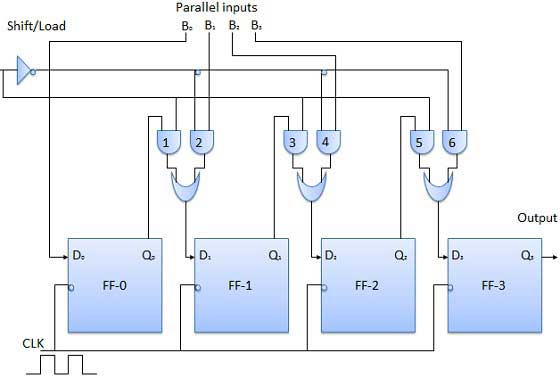
The circuit, shown below, is a four-bit parallel-in serial-out register.
-
Output of the previous flip Flop is connected to the input of the next one via a combinational circuit.
-
The binary input data bits B0, B1, B2, B3 are applied through the same combinational logic circuit.
-
There are two modes in which this circuit can work, namely - shift mode and load mode.
Load mode
When the shift/load bar line is low (0), the AND gates 2, 4 and 6 become active, and they will pass B1, B2, B3 bits to the corresponding flip-flops. On the low going edge of the clock, the binary inputs B0, B1, B2, B3 will get loaded into the corresponding flip-flops. Thus, the parallel loading takes place.
Shift mode
When the shift/load bar line is low (1), the AND gates 2, 4 and 6 become inactive. Hence, the parallel loading of the data becomes impossible. But the AND gates 1,3 and 5 become active. Therefore the shifting of data takes place from left-to-right bit-by-bit on the application of clock pulses. Thus, the parallel-in serial-out operation takes place.
Block diagram
