Applications of shift registers
Table of contents
Overview
Shift registers are sequential circuits used primarily used for:
- Storage of Data
- Data transfer through movement of binary data
- Data manipulation
- Counter implementation
They are called shift registers as it moves or shifts binary input data to its output per clock cycle. Shift registers are commonly used to store data inside calculators. Even in computer systems, operations like addition, subtraction, division and multiplication are performed by registers.
Shift registers can be applied in the following ways:
-
Parallel to Serial conversion: Used in transmitters after analog to digital conversion in order to convert parallel input data into serial data
-
Serial to Parallel conversion: Used in receivers before digital to anlogous conversion takes place in order to convert serial input data into parallel data
-
Sequence Generator: Generate a sequence of 0s and 1s when combined with some additional gates
-
Counters: Shift registers can be implemented as counters based on the output of the rightmost D flip-flop that is connected to the serial input, namely the Ring Counter and the Johnson Ring Counter
-
Serial-in Serial-out registers are used for time delays
Ring counter
Similar to how the Serial-in Serial-out register requires ‘N’ clock pulses to shift N bit data, the ‘N’ Ring Counter produces a sequence of 0s and 1s, by having the rightmost D flip-flop as input to the leftmost D flip-flop as opposed to applying data externally. That is, the output of the last flip-flop is connected to the output of the first flip-flop in the ring. These patterns of states (0s and 1s) are repeated every ‘N’ clock cycles.
The number of states in a Ring Counter are directly proportional to the number of flip-flops used.
The block diagram of the 3-bit Ring counter is shown in the following figure.
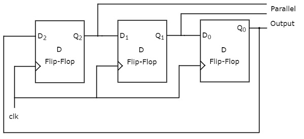
A 3-bit Ring Counter will contain only a 3-bit SIPO shift register.
Assume, the initial status of the D flip-flops from leftmost to rightmost is Q2Q1Q0=001. Here, Q2 & Q0 are MSB & LSB respectively. You can understand the working of Ring counter from the following table.
| No of positive edge of Clock | Serial Input = Q0 | Q2(MSB) | Q1 | Q0(LSB) |
|---|---|---|---|---|
| 0 | - | 0 | 0 | 1 |
| 1 | 1 | 1 | 0 | 0 |
| 2 | 0 | 0 | 1 | 0 |
| 3 | 0 | 0 | 0 | 1 |
Due to the absence of the clock signal, the initial status of the D flip-flops is Q2Q1Q0=001. This state will repeat every third positive edge transition of the clock signal.
Similarly, the following operations take place every positive edge of the clock cycle:
-
Serial input of the first D flip-flop gets the previous output of the third flip-flop. Thus, the present output of the first D flip-flop is equal to the previous output of the third flip-flop.
-
The previous outputs of first and second D flip-flops are right-shifted by one bit. That implies that the present outputs of second and third D flip-flops are equal to the previous outputs of first and second D flip-flops.
Johnson ring counter
The Johnson ring counter functions similarly to the Ring counter. The difference being that the complemented output of rightmost D flip-flop is given as input of leftmost D flip-flop instead of normal output. Thus, ‘N’ bit Johnson Ring counter produces a sequence of states (pattern of zeros and ones) and it repeats for every ‘2N’ clock cycles.
Johnson ring counter is also called the Twisted ring counter and Switch tail ring counter. The block diagram of 3-bit Johnson Ring counter is shown in the following figure.
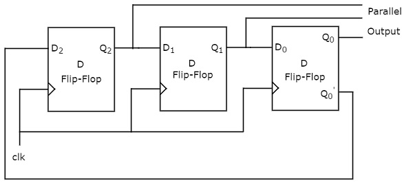
The 3-bit Johnson Ring counter also contains only a 3-bit SIPO shift register.
Assume, initially, all the D flip-flops are cleared. So, Q2Q1Q0=000. Here, Q2 is the MSB & Q0 is the LSB.
| No of positive edge of Clock | Serial Input = Q0 | Q2(MSB) | Q1 | cQ0(LSB) |
|---|---|---|---|---|
| 0 | - | 0 | 0 | 0 |
| 1 | 1 | 1 | 0 | 0 |
| 2 | 1 | 1 | 1 | 0 |
| 3 | 1 | 1 | 1 | 1 |
| 4 | 0 | 0 | 1 | 1 |
| 5 | 0 | 0 | 0 | 1 |
| 6 | 0 | 0 | 0 | 0 |
The initial status of the D flip-flops in the absence of the clock signal is Q2Q1Q0=000. This status repeats for every six positive edge transitions of the clock signal.
Similarly, the following operations take place for every positive edge of the clock signal.
- Serial input of first D flip-flop gets the previous complemented output of the third flip-flop. So, the present output of the first D flip-flop is equal to the previous complemented output of the third flip-flop.
- The previous outputs of first and second D flip-flops are right shifted by one bit. That means, the present outputs of second and third D flip-flops are equal to the previous outputs of first and second D flip-flops.